Saturday, 21 January 2017

Using the Digital Clock Manager

One of the other resources on the Spartan 3E FPGA is the Digital Clock Manager. These are very handy!

What are Digital Clock Managers?

DCMs receive an incoming clock and can do the following and more:

• Generate a faster or slower clock signal using an input clock as a reference
• Generate signals with a known phase shift (e.g., 90, 180 or 270 degrees out of phase)
• Correct clock duty cycles, ensuring that the high and low times are 50%
• Phase shift the internal FPGA clock signals to compensate for internal clock distribution delays

DCMs can also be cascaded, allowing multiple clocks to be used. For example, one external 50MHz clock can be used to generate 100MHz controlling memory and 25MHz for the VGA pixel clock.
Because of this flexibility they are quite complex to use. I find using the CORE Generator is the best way to configure a DCM.

Using the Wizard

Pick any project you like, and add a "New Source", using the "IP (CORE Generator. . . )" option to create a component "my_dcm":


Once again choose the "Only IP compatible with chosen part" option, then drill down to "Single DCM_SP":


Click "Next" then "Finish" to start the CORE Generator.
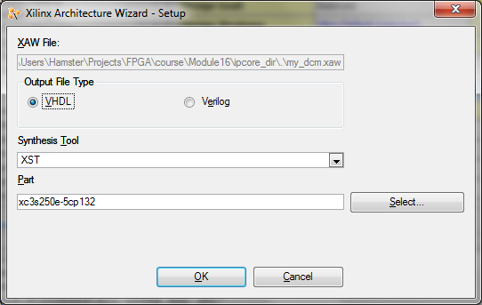
You will then be presented with this dialog box:


Just click "OK" to open the Clocking Wizard’s General Setup dialogue box:

Here you can choose what signals you will use and set the input clock frequency. The most common output I use is the CLKFX (which is the synthesized output frequency). You may want to untick the RST (reset) signal if this is the only clock for the entire project:


The next screen allows you to choose what clock buffers are being used. For most projects you will use "Global Buffers" - being global the clock signal is available to all logic on the FPGA:


The next screen is the interesting one - it’s where you get to set the output frequency. Input the desired frequency and press "Calculate":


You will now get the summary screen, where you can click "Finish":


Once generated, you will be able to use the instantiation templates to add a "my_dcm" component to your project.

Project - Use a DCM

• Add a DCM to one of your projects

Note

Remember to update not only the signal monitored by rising_edge(), but also the signal used on the process sensitivity list.

Friday, 20 January 2017

Implementing Finite State Machines

Up to now the projects have been very linear - mostly counters that work like clockwork. Now we are going to investigate how you can get your logic to allow external signals change it’s behaviour, rather than just processing the results. The technique introduced is used in many different areas of a design, such as:
• Communication protocols, where data may be sent asynchronously or different data required different responses
• Scheduling of control signals in a memory controller
• Decoding and executing instructions in a CPU
• Control of simple machine
• Implementing simple user interfaces

Introduction to the project

For the project we are going to build a combination lock, which works as follows:

• All of the switches must be turned off
• Then switch 7 must be turned on
• Then switch 6 must be turned on
• Then switch 5 must be turned on
• Finally switch 4 must be turned on

If this sequence is followed, all the LEDs will turn on and stay on until all switches are moved back to off.

In software this would be quite easy - using the console for user input something like this would be quite close :

while(1)
{
if(getchar() = ’7’ && getchar() = ’6’ && getchar() = ’5’ && getchar() = ’4’)
{
LEDs = 0xFF;
getchar();
}
}

To get the same result, we need to use a finite state machine (FSM) - a directed graph of states and how the system moves between the states. There is a formalized way to document FSMs, but here’s my somewhat less formal approach which works well when sketching designs on paper


At any point in time your design is at a state indicated by a circle. On the next clock tick ”it must” follow an arrow. All options ”must” be mutually exclusive. I have added bold arrows to indicate the "no other arrow applies" option.

So when the system is in the "START" state the options are either:

• If switches are set to "0000000" we go to the "START" state.
• If switches are set to "1000000" we go to the "ONE RIGHT" state.
• Otherwise we go to the "ERROR" state.
Likewise, in the "ERROR" state the options are:
• If switches are set to "0000000" we go to the "START" state.
• Otherwise we go to the "ERROR" state.

 Implementing in VHDL

Implementation is relatively easy.

You can either use enumerated types (that have not been covered), but it is usually better to use constants:
...
constant state_error : STD_LOGIC_VECTOR(3 downto 0) := "0000";
constant state_start : STD_LOGIC_VECTOR(3 downto 0) := "0001";
constant state_one_right : STD_LOGIC_VECTOR(3 downto 0) := "0010";
...
signal state : STD_LOGIC_VECTOR(3 downto 0) := (others => ’0’);

If you use constants, then you can encode output signals within the states, ensuring that you get glitch-less signals. If you like, you could include this in your project to help with debugging:

leds(3 downto 0) <= state;

In your project’s process it is usually easiest to code it using a CASE statement like this:

if rising_edge(clk) then
case state is
when state_error =>
case switches is
when "00000000" => state <= state_start;
when others => state <= state_error;
end case;
when state_start =>
case switches is
when "00000000" => state <= state_start;
when "10000000" => state <= state_one_right;
when others => state <= state_error;
end case;
when state_one_right =>
case switches is
when "10000000" => state <= state_one_right;
when "11000000" => state <= state_two_right;
when others => state <= state_error;
end case;
....
when others =>
state <= state_error;
end case;
end if;

Project - Combination lock 1

• Code the above FSM to implement the combination lock. To give some feedback on success set LEDs to "11111111", and
• Test it in the simulator, using this in the testbench stimulus process

switches <= "00000000";
wait for 200 ns;
switches <= "10000000";
wait for 200 ns;
switches <= "11000000";
wait for 200 ns;
switches <= "11100000";

If I have designed it correctly, the only way to get to the "OPEN" state is to move the switches through "00000000", "10000000", "11000000", "11100000", then finally to "11110000"

wait for 200 ns;
switches <= "11110000";
wait for 1000 ns;
switches <= "00000000";

• Try running it in hardware - it most probably won’t work reliably - 50:50 if you are lucky.

The problem with switch bounce

This design will work perfectly well - as long as the switch contacts don’t bounce. If they bounce the FSM will view that as an "otherwise" case and go to the error state.

Solutions are:

• Debounce the switches in hardware
• Debounce the switch signals using logic within the FPGA
• Sample the switches at intervals that should mask any bounce - perhaps every 1/10th of a second
• Update the FSM to allow for switch bounces

The "debounce" solutions are all relatively hard, while updating the FSM will only need a few lines of code.

Project - Combination lock 2

• Trace through the FSM diagram to work out why a bounce causes it to fail
• Update the FSM to ignore switch bounces

If you wish, test it in the simulator - here is stimulus that looks like four bouncing switches:

switches <= "00000000";
wait for 200 ns;
switches <= "10000000";
wait for 50 ns;
switches <= "00000000"; -- bounce
wait for 50 ns;
switches <= "10000000";
wait for 300 ns;
switches <= "11000000";
wait for 50 ns;
switches <= "10000000"; -- bounce
wait for 50 ns;
switches <= "11000000";
wait for 300 ns;
switches <= "11100000";
wait for 50 ns;
switches <= "11000000"; -- bounce
wait for 50 ns;
switches <= "11100000";
wait for 300 ns;
switches <= "11110000";
wait for 50 ns;
switches <= "11100000"; -- bounce
wait for 50 ns;
switches <= "11110000";
wait for 1000 ns;
switches <= "00000000";

• Test it in hardware

Challenges

• Can you make the LEDs flash off and on for a few seconds when an error occurs?
• Can you make the board flash the LEDs in a pattern stored in BRAM when it reaches the "OPEN"

Generating analogue signals

One of the nice features of FPGAs is how flexible the I/O pins are. In this chapter we will make a standard I/O pin generate an analogue signal, playing a tone using a waveform that is stored in block RAM.
This module is largely based on Xilinx’s AppNote xapp154.pdf.

One bit (Delta Sigma) DAC

You are most probably familiar with Pulse Width Modulation (PWM), when a signal of a constant frequency has its duty cycle modulated to generate different power levels. If a PWM signal is passed through a low pass filter you end up with an analogue voltage that is proportional to the duty cycle. PWM is used in power supplies, light dimmers and motor controllers and such.

Delta Sigma modulation is a lot like that, but without the constant frequency of PWM. It has an output that hunts for the desired output value. A one bit DAC has only two output values (1 or 0), and it generates the value which when included in a running average brings it closest to the desired level:
• To generate a level of 0.5 the output will be "10101010101. . . "
• To generate 0.25 the output will be "000100010001. . . "
• To generate 0.66 the output will be "110110110110110. . . "
All of these signals average out to the desired value but have different frequencies.

Um, that looks really hard to do

It’s not that hard at all. For this example, work in decimal to make it clearer, but implementation in binary is just the same.

To make a Delta Sigma DAC with 100 output levels you need an accumulator with two decimal digits, and you use the "carry to the hundreds" as the output. Just keep adding the desired output level to the two digits and the "carry to the hundreds" will be a stream of ones and zeros that averages to the desired level.

Here’s a two decimal digit DAC generating the output of 33:

Iteration             Digits                  Carry/Output
0                          50                           0
1                          83                           0
2                          16                           1
3                          49                           0
4                          15                           1
6                          48                           0
7                          81                           0

Pretty simple!
Of course there are a few little tricks:
• Do it quick enough so that at the highest required frequency you have enough \’1’s and \’0’s to average over
• Careful design of an analogue output filter is required for best performance
• Do not use all the DAC’s range, as the spectrum of noise at either end is problematic

Rough back-of-the-envelope bandwidth and effective resolution calculation

If you need to produce signals at 22kHz, you have to use at least a 44kHz playback frequency. If the one-bit DAC runs at 25MHz there is a just over five hundred output values (ones and zeros) per 1/44000th of a second at best you have nine-bit resolution at that frequency.

Doing it in VHDL

Here is the code for an 8 bit DAC. It is pretty much a "count by n" counter:

library IEEE;
use IEEE.STD_LOGIC_1164.ALL;
use IEEE.STD_LOGIC_ARITH.ALL;
use IEEE.STD_LOGIC_UNSIGNED.ALL;
entity dac8 is
Port ( Clk : in STD_LOGIC;
Data : in STD_LOGIC_VECTOR (7 downto 0);
PulseStream : out STD_LOGIC);
end dac8;
architecture Behavioral of dac8 is
signal sum : STD_LOGIC_VECTOR (8 downto 0);
begin
PulseStream <= sum(8);
process (clk, sum)
begin
if rising_edge(Clk) then
sum <= ("0" & sum(7 downto 0)) + ("0" &data);
end if;
end process;
end Behavioral;

Connecting up the headphones

On the Papilio One, just plug amplified speakers into the jack and use the following constraint:
Constraint for the Papilo One
NET "Audio" LOC = "P41";

Connecting headphones to the Basys2

Unlike the Papilio One + LogicStart MegaWing combo the Basys2 does not have an audio output, so we need to use a PMOD port. The PMODs on the Basys2 board have four signal wires from the FPGA, a ground and a 3.3V power connection. For the JA header on the Basys2 board the constraints are:
Contraints for the Basys2

NET "JA<0>" LOC = "B2";
NET "JA<1>" LOC = "A3";
NET "JA<2>" LOC = "J3";
NET "JA<3>" LOC = "B5";

Caution

Make sure that you don’t short the power pins. Shorting out ground and power will upset your USB port and/or your FPGA board

For this project connect a set of stereo earphones between pin 0 and pin 1 and the ground. To do this I used a header strip, 3.5mm jack and a length of wire:


If you pull the unused pins out of the header strip you might just be able to hold the 3.5mm jack in place at the correct time. . .

The inductive nature of the headphones/earphones proves to be a pretty good low pass filter for the high frequency signals so no additional components are needed - but if you want to you can include a suitable capacitor in series to prevent average DC voltage running through them.

The Basys2 board has a 200 ohm resistor in series with the FPGA output pin. This makes the PMOD connectors somewhat protected against ESD, overvoltage and shorts. For this project it also acts as a voltage divider reducing the DC bias and the peak to peak voltages that go through the headphones/earphones.

Project - Wave file generation

In the prior project we hooked a block RAM to the LEDs, and used it to flash them. We can do the same to generate an audio waveform.
• Make a COE file containing the samples for a sine wave (something like "f(n) int((sine(n*PI()/1024)+1)*100)+128" will give you values between 28 and 228 that you can use).
• Load it into the flashylights project and check that the lights look OK.
• To generate an audible tone we need to cycle through this somewhere around 400 times per second - so we need to use counter(15 downto 6) to address the ROM component. This should generate a tone of one cycle every 65536 clocks = 381.4Hz
• Add an 8 bit DAC to your project and connect it to the audio output. Remember to add the appropriate constraints to your project!
• Build and download the design. If you connect your headphones you should have a tone!

 Challenges

• At the moment we can only generate one frequency. Design and try out ways to make different frequencies.
• The Spartan 3E-250 has 24K of on-chip memory. That’s enough for 2 seconds of telephone quality 11kHz/8 bit audio. . . .
• If you connect the two high address bits on RAM to switches you can have four different waveforms, each with 256 samples per cycle, possibly allow you to generate Square, Saw, Ramp and Sine waves from one project.
• By right-shifting the samples you can control the volume - and with a wider DAC you can keep the least significant bits. Remember to sign-extend the sample when you shift it (e.g. y(8 downto 0) = x(7) & x(7 downto 0)).
• The design is quite lo-fi - very 8 bit! You could extend the DAC to 16 bits, and of course changing the ROM to have a data width of 16 (you will also need a new .coe file with samples expanded out to match the range of the 16 bit values).

Wednesday, 18 January 2017

Using the FPGA’s internal RAM

As well as the resources required for implementing digital logic, FPGAs also have a small amount of RAM built in. This RAM is very useful and can meet the entire RAM needs of many projects.

Each Vendor’s RAM blocks have differing capabilities and is configured differently, so it makes sense to use this as a way of introducing the IP Core Generator.

This project is very "GUI" based - unlike the last module it is very much a walk through.

What is Block RAM? What can it do?

On the Spartan 3E each RAM block has 18 kilobits of RAM, and can be presented to the system in different widths. Eighteen kilobits is an odd size, but it is designed that way to allow for either parity or ECC bits to be stored.

The most common configuration I’ve used is 2048 words of 8 bits, but it can be configured as one of either 16k x 1bit, 8k x 2 bits, 4k x 4 bits, 2k x 8 bits, 2k x 9 bits, 1k x 16 bits, 1k x 18 bits, 512 x 32 bits, 512 x 36 bits or 256 x 72 bits.

The blocks are especially useful as they are dual-port - there are two independent address, read and write ports that simplify many designs (such as building FIFOs).

Using the CORE Generator with BRAM

Using the CORE generator makes building BRAM components very simple - and if required it also transparently constructs larger memories out of multiple primitives. In the project you will use the CORE Generator as creating them directly in VHDL is quite cumbersome and complex.

Preparing the project

• Create a new project - I called mine "flashylights".
• Add a module which has the clock signal as the only input and the eight LEDs as the output
You should get a module that looks like this:
library IEEE;
use IEEE.STD_LOGIC_1164.ALL;
entity FlashyLights is
Port ( clk : in STD_LOGIC;
LEDs : out STD_LOGIC_VECTOR (7 downto 0));
end FlashyLights;
architecture Behavioral of FlashyLights is
begin
end Behavioral;

We now need to add a couple of Wizard generated components.

Using the IP CORE Generator

Add a new source file to the project:

Select "IP" and call the module counter30 - it will be a 30 bit counter

You will be presented with the "Select IP" dialogue box. Tick the "Only IP compatible with chosen part" tickbox:


Navigate down into "Basic Elements"/"Binary Counter" and click "Next"

After a long delay, the options for Binary Counter will appear. Set the "Output Width" to 30 - and if you want, click on the "Datasheet" button:

Then click "Generate".
In the Hierarchy window you will now have a "counter30" component. Click on it and then under the Processes tree select "View HDL Instantiation Template":


Copy and paste the useful bits into your top level project - add a signal "counter" to be connected to the output of the counter.  Here’s the completed source:

library IEEE;
use IEEE.STD_LOGIC_1164.ALL;
entity FlashyLights is
Port ( clk : in STD_LOGIC;
LEDs : out STD_LOGIC_VECTOR (7 downto 0));
end FlashyLights;
architecture Behavioral of FlashyLights is
COMPONENT counter30
PORT (
clk : IN STD_LOGIC;
q : OUT STD_LOGIC_VECTOR(29 DOWNTO 0)
);
END COMPONENT;
signal count : STD_LOGIC_VECTOR(30 downto 0);
begin
addr_counter : counter30
PORT MAP (
clk => clk,
q => count
);
end Behavioral;

Adding the ROM component

Add another new IP module called "memory", but this time select the Block Memory Generator:


The Block Memory Generator has 6 pages of settings - at the moment we only need to enter things on the first three. Just click "Next" on the first screen:


Select that we want a Single Port ROM, then click "Next":


Set "Read Width" to 8 - we have eight LEDs to light. Set the "Read Depth" to 1024. Click "Next":


Don’t bother going through the rest of the screens - they don’t apply at the moment - just click "Generate"
You will now have another component, and you can view its instantiation template.


Add it to the source, connecting the top 10 bits of the counter to the ROM’s address bus (addra), and the data bus (douta) to the LEDs:

library IEEE;
use IEEE.STD_LOGIC_1164.ALL;
entity FlashyLights is
Port ( clk : in STD_LOGIC;
LEDs : out STD_LOGIC_VECTOR (7 downto 0));
end FlashyLights;
architecture Behavioral of FlashyLights is
COMPONENT counter30
PORT (
clk : IN STD_LOGIC;
q : OUT STD_LOGIC_VECTOR(29 DOWNTO 0)
);
END COMPONENT;
COMPONENT memory
PORT (
clka : IN STD_LOGIC;
addra : IN STD_LOGIC_VECTOR(9 DOWNTO 0);
douta : OUT STD_LOGIC_VECTOR(7 DOWNTO 0)
);
END COMPONENT;
signal count : STD_LOGIC_VECTOR(29 downto 0);
begin
addr_counter : counter30
PORT MAP (
clk => clk,
q => count
);
rom_memory: memory
PORT MAP (
clka => clk,
addra => count(29 downto 20),
douta => LEDs
);
end Behavioral;


Once built, you can view the RTL schematic - looks as you would expect:


Setting the contents of the ROM

At the moment the ROM is blank (all ’0’s). When the FPGA is configured, the contents of the block RAM can be set to values that are predefined in the configuration bit stream.

Page 4 of the Block Memory Generator gives you the option to set the contents of the ROM using a ".coe" file. Here’s enough of the file that you will be able to write your own from scratch:

memory_initialization_radix=10;
memory_initialization_vector=
128,
128,
127,
127,
127,

Here’s another, using binary (as memory_initialization_radix=2) for a memory with a data width of 15:
memory_initialization_radix=2;
memory_initialization_vector=
001110000000001,
010110000000010,
000010000000011,
000010000000100,
000010000000101,
000010000000110,

Create a sample file of 8 bit binary values - make the 1 bits zig-zag from left to right, or some other pattern - the more lines the merrier. Call it "flashy.coe".

Edit the "memory" component (just double-click it in the Hierarchy tree) and skip through to Page 4. Set the initialisation file to flashy.coe.


It is always a good idea to click on the "Show" button - it will give you a warning if your .coe file is not correct. Click the Generate button to update the IP module.

As an aside, there are other ways to do this, allowing you to inject contents (e.g., maybe bootloader) after the .bit file is built. This allows you to avoid a lengthy rebuild of a whole project just to change the initial values in a BRAM. It is also a good way to allow an end-user to customise the .bit file without providing access to your source code. Search for "Xilinx data2mem" on Google.

The finishing touches

NET LEDs(7) LOC = "P5" | IOSTANDARD=LVCMOS25;
NET LEDs(6) LOC = "P9" | IOSTANDARD=LVCMOS25;
NET LEDs(5) LOC = "P10" | IOSTANDARD=LVCMOS25;
NET LEDs(4) LOC = "P11" | IOSTANDARD=LVCMOS25;
NET LEDs(3) LOC = "P12" | IOSTANDARD=LVCMOS25;
NET LEDs(2) LOC = "P15" | IOSTANDARD=LVCMOS25;
NET LEDs(1) LOC = "P16" | IOSTANDARD=LVCMOS25;
NET LEDs(0) LOC = "P17" | IOSTANDARD=LVCMOS25;
NET "clk" LOC="P89" | IOSTANDARD=LVCMOS25 | PERIOD=31.25ns;

Rebuild the project, download it and watch the lights!

Tuesday, 17 January 2017

A better display than LEDs

Now is a good time to cover a little more VHDL, and use it to efficiently implement a design that controls the seven segment display.

The VHDL case statement

Much like "switch()" in C, VHDL has the CASE statement that allows you to choose between multiple different paths through your code based on the value of a signal. Although it is largely functionally equivalent to nested ’IF’s it is far easier to write, and is implemented more efficiently within the FPGA.

It looks much like this:

CASE input(2 downto 0) IS
WHEN "000" =>
output1 <= ’1’;
output2 <= ’1’;
WHEN "001" =>
output1 <= ’0’;
output2 <= ’1’;
WHEN "110" =>
output1 <= ’1’;
output2 <= ’0’;
WHEN OTHERS =>
output1 <= ’0’;
output2 <= ’0’;
END CASE;

It differs from most similar constructs in programming languages in that all possible cases must be covered, so it pays to remember that a STD_LOGIC signal can have other states than just ’1’ or ’0’ - most designers choose to use the ’least harmful’ actions on an unexpected value. Like an "IF" statement, "CASE" can only be used inside a process - and remember to include the signals being tested in the process’s sensitivity list when a "CASE" statement is used outside of an "IF RISING_EDGE(clk) THEN" block.

Note that a CASE block must be inside a PROCESS block.

Excellent practice for using the CASE statement is driving the seven segment display - you can use it twice. One CASE statement decodes which segments to light, and a second CASE statement selects which digit is active at any time.

Project - Displaying digits

These projects are a lot of work and might take a couple of sittings, but you will build up a great understanding of the seven segment displays. If you are feeling confident, combine a few of the steps and race through.

• Add "anodes(3 downto 0)" and "sevenseg(6 downto 0)" as outputs to your top level design, and then add the following constraints
to your ucf file:

# Constraints for Papilio One
NET "anodes<0>" LOC="P18";
NET "anodes<1>" LOC="P26";
NET "anodes<2>" LOC="P60";
NET "anodes<3>" LOC="P67";
NET "segments<6>" LOC="P62";
NET "segments<5>" LOC="P35";
NET "segments<4>" LOC="P33";
NET "segments<3>" LOC="P53";
NET "segments<2>" LOC="P40";
NET "segments<1>" LOC="P65";
NET "segments<0>" LOC="P57";
NET "dp" LOC="P23";
# Constraints for the Basys2
NET "sevenseg<0>" LOC = "L14";
NET "sevenseg<1>" LOC = "H12";
NET "sevenseg<2>" LOC = "N14";
NET "sevenseg<3>" LOC = "N11";
NET "sevenseg<4>" LOC = "P12";
NET "sevenseg<5>" LOC = "L13";
NET "sevenseg<6>" LOC = "M12";
NET "dp" LOC = "N13";
NET "anodes<3>" LOC = "K14";
NET "anodes<2>" LOC = "M13";
NET "anodes<1>" LOC = "J12";
NET "anodes<0>" LOC = "F12";

• In your top level design, connect the outputs sevenseg and dp directly to the inputs from the switches. Within your design set anodes to "1110" then build the design. As the anodes are "active low" this value should enable only the rightmost digit of the sevenseg displays.
• Work out and document the switch patterns required to give the digits 0 through 9, and the letters A through F.
• Build a CASE statement to decode the binary of switches(3 downto 0) and display it on the first seven segment display - remember that at least switches(3 downto 0) has to be included in the sensitivity list of the process acting on them, as there is no clock being used.

Multiplexing digits

If each digit is displayed in quick succession the eye can be fooled into seeing all four displays as being lit at the same time. As we have four digits we can use two bits of a suitably sized counter to select which is to be lit. If the design switches digits too fast it will not give them enough time to light up, and too slow will cause flickering. Something around 200Hz to 1kHz seems to work best.

Counter bits               Value for anodes                           Values for sevenseg()
00                                   1110                                                 Digit 0
01                                   1101                                                 Digit 1
10                                   1011                                                 Digit 2
11                                   0111                                                  Digit 3

You can either decide to decode the four digits in each option of the CASE statement (using nested CASE statements), or maybe create a signal "thisdigit : STD_LOGIC_VECTOR(3 downto 0)" with the digit to be decoded within the case, and then just decode that signal.

Project - Using the Seven segments

• Update your project to multiplex all four displays and show the values of switches(3 downto 0) on all digits
• Update your project to multiplex all four displays and show the value of switches(3 downto 0) on digits 0 and 1, and the value of switches(7 downto 4) on digits 2 and 3
• Update your project to show the highest 16 bits of a counter over all four digits.
• Create a new module that can display four digits on the seven segment display. This will be useful for any project you design that uses the sevenseg displays. Its interface signals should look something like:
clk : in std_logic
digit0 : in std_logic_vector(3 downto 0)
digit1 : in std_logic_vector(3 downto 0)
digit2 : in std_logic_vector(3 downto 0)
digit3 : in std_logic_vector(3 downto 0)
anodes : out std_logic_vector(3 downto 0)
sevenseg : out std_logic_vector(6 downto 0)
dp : out std_logic

Challenges

• Can you make the display count only in decimal rather than hexadecimal?
• Can you make the display count in minutes and seconds?

Monday, 16 January 2017

Using more than one module in a design

Up to now the designs have consisted of only one entity. Just like in software, there quickly comes a time when putting every statement in one source file is no longer practical. There is also the need to separate designs into functional units that can be designed and tested independently of each other, before they are integrated into one design.

In VHDL speak, these are called modules.

Using more than one source module in a design

VHDL achieves this through "architectures", "components", "entities" and "instances" - we have already breezed over all of this.

• The "entity" statement defines the inside view of a module’s interface:
entity mymodule is

Port ( input1 : in STD_LOGIC_VECTOR (3 downto 0);
output1 : out STD_LOGIC_VECTOR (3 downto 0));
end mymodule;

This is at the top of the defining module, following the "use" statements.

• The "architecture" statement defines how a component works - it contains all the internal signals and sub-components, and all the internal logic:

architecture Behavioral of mymodule is
begin
output1 <= input1;
end Behavioral;

This is usually the bulk of the module, and appears after the entity statement.

• The "component" statement defines the ’external’ connections of the module, and appears in the module that uses the component:

COMPONENT mymodule
PORT(
input1 : IN std_logic_vector(3 downto 0);
output1 : OUT std_logic_vector(3 downto 0));
END COMPONENT;

Component declarations appear in the same area of the code as the signal declarations.

• The "instance" statement describes the connections of the component inside the containing module - it is this that actually triggers the component to be included in the final design:

Inst_mymodule: mymodule PORT MAP(
input1 => input_signal1,
output1 => output_signal1
);

These can be intermingled with the assignment statements and processes, but not contained within a process block. One source of frustration for me is that when signals are mapped they cannot be operated on (e.g., input_a ) signal_a is valid but input_a ) NOT(signal_a) is not). All inputs should have a value, but if you don’t want to use an output, you can map it to the keyword "open" (e.g., "output1)open").

Creating a module using the wizard

The easy way to create a new module is by using the "New Source" wizard.
On the first screen, give the module a name:


Then define the interface - do not worry if you are not 100% sure of the signals, you can change them directly in the source afterwards:


You are then presented with a summary screen, and can then click ’Finish’.
Once you have a new module, you can highlight it, and under "Design Utilities" you can run the "View HDL Instantiation Template" process to get a template that you can cut and paste as needed:


It will look something like this:

COMPONENT mymodule
PORT(
input1 : IN std_logic_vector(3 downto 0);
output1 : OUT std_logic_vector(3 downto 0)
);
END COMPONENT;
Inst_mymodule: mymodule PORT MAP(
input1 => ,
output1 =>
);

In most large designs the very top level module ends up containing very little logic and resembles a big wiring loom - with a lot of instances of smaller components and the signals that interconnect them.

Project


• Create a new module - a 30-bit counter called "counter30", with the following external signals:
– clk : in STD_LOGIC
– enable : in STD_LOGIC
– count : out STD_LOGIC_VECTOR(29 downto 0)
The internal design is up to you, but your earlier counter project will be pretty close.
• View the ’Instantiation Template’ for your component. Copy the component declaration into your switches_leds.vhd source
• In switches_leds create an instance of counter30
– Connect the counter’s count output to a bus called count1
– Connect the "enable" signal to switch(0)
– Connect the clock
– Connect the top four bits of count1 to LEDs(3 downto 0). Remember to add a signal definition for count1
• Implement the design and test that it works as expected - switch 0 should enable the counter driving the lower four LEDs. It is usual to get a lot of warnings about unused signals that will be trimmed from the design. This is expected as we are only using the top four bits of the counters.
• Create a second instance of counter30 in the switches_leds vhd source
– have its count output connected to a bus called count2
– connect the "enable" signal to switch(1).
– connect the top four bits of count2 to LEDs(7 downto 4)
• Check that this too works as expected.


Using the ISIM simulator

Now that we have a design that changes millions of times a second, testing becomes hard. In this module we will use the ISIM simulator - a tool that allows you to ’run’ the logical design and see how it behaves as it is poked and prodded with external signals.

What is simulation?

When you debug software you are actually running the code on the processor, with all the access to the system resources such as the OS, memory, communications and file systems. Unlike debugging software, simulating an FPGA project doesn’t run it on the actual hardware - the closest equivalent you may have experience with is the simulation of a microcontroller in MPLAB or WinAVR.

Although no FPGA hardware is involved, simulation is very powerful - it is very much like having the most powerful logic analyser at your fingertips. The downside is that if your idea of how an external device works isn’t accurate you will not be able to spot the problems.

The initially confusing bit about simulation is that it requires another VHDL module to drive the input signals and receives the outputs from your design - a module that is called a "test bench". They are pretty easy to spot - the ENTITY declaration has no "IN" or "OUT" signals, just something like this:

ENTITY TestBench IS
END TestBench;

In effect, the test bench is a module that ties up all the loose ends of your design so that the simulator can run it.

Creating a test bench module

Here is how to create a test bench using the wizard in WebPack.

Right-click on the top level of the hierarchy and select to add a new source module into the project:


Select the "VHDL Test Bench" and assign it a name (I just add tb_ to the name of the component being tested), then click ’Next’:


You will then need to select which component of the design you wish to test and then click ’Next’:


A summary screen will be presented - review the details and then click ’Finish’.

Breakdown of a Test Bench module

Here is the resulting VHDL with most of the comments removed, to reduce its size:

LIBRARY ieee;
USE ieee.std_logic_1164.ALL;
ENTITY tb_Switches_LEDs IS
END tb_Switches_LEDs;
ARCHITECTURE behavior
COMPONENT Switches_LEDs
PORT(
switches : IN std_logic_vector(7 downto 0);
LEDs : OUT std_logic_vector(7 downto 0);
clk : IN std_logic
);
END COMPONENT;
--Inputs
signal switches : std_logic_vector(7 downto 0) := (others => ’0’);
signal clk : std_logic := ’0’;
--Outputs
signal LEDs : std_logic_vector(7 downto 0);
-- Clock period definitions
constant clk_period : time := 20 ns;
BEGIN
-- Instantiate the Unit Under Test (UUT)
uut: Switches_LEDs PORT MAP (
switches => switches,
LEDs => LEDs,
clk => clk
);
-- Clock process definitions
clk_process :process
begin
clk <= ’0’;
wait for clk_period/2;
clk <= ’1’;
wait for clk_period/2;
end process;
-- Stimulus process
stim_proc: process
begin
wait for 100 ns;
wait for clk_period*10;
wait;
end process;
END;

This has a few more language structures that have not been seen so far. First is a component declaration, which defines the project that is being tested - much like a C function prototype:

COMPONENT Switches_LEDs
PORT(
switches : IN std_logic_vector(7 downto 0);
LEDs : OUT std_logic_vector(7 downto 0);
clk : IN std_logic
);
END COMPONENT;
There is a "constant" declaration, which is of a "time" data type - this data type is exclusively used in simulation. If your design has a timing constraint, the value here is usually set correctly, but it pays to check:
constant clk_period : time := 20 ns;

The next stanza is creating an instance of the Switches_LEDs component, and attaching its signals to the signals within the test bench:

uut: Switches_LEDs PORT MAP (
switches => switches,
LEDs => LEDs,
clk => clk
);

And finally, two processes that contain "wait" statements. These two processes control the timing of signals within the simulation:

clk_process :process
begin
clk <= ’0’;
wait for clk_period/2;
clk <= ’1’;
wait for clk_period/2;
end process;
-- Stimulus process
stim_proc: process
begin
wait for 100 ns;
wait for clk_period*10;
wait;
end process;

The first process (clk_process) defines the clock signal - which will stay 0 for ten (simulated) nanoseconds, then flip to 1 for ten nanoseconds - giving a 20ns (50MHz) clock. The second process (stim_proc) is where you add statements to change the inputs of the unit under test - for example, you could use "switches ( "11111111" to simulate the switches being turned on. When initially created, all inputs (other than the clock signal) are set to 0.

Warning

The "wait for [time period]" cannot be realized inside an FPGA, so it is only useful inside simulations. If you use this statement outside of a testbench your design will simulate perfectly but you will not be able to implement your design in the FPGA.

Starting the simulation

From top to bottom, switch to "Simulation" view, select the desired test bench (you can have more than one), expand the "Processes" tree, and then double-click on "Simulate Behavioral Model" - as a quirk, if you have just finished a simulation, you may need to right-click on this and choose "Run all".

The simulation will be compiled, and then the simulator tool is launched. On start-up the simulator will simulate the first microsecond:


Using the simulator

From left to right you have the following panes:
• Instances and processes - the design hierarchy being simulated
• Objects - what signals are in the selected instance
• Waveform window - a list of signals being recorded, and a graphical display of their values over time

Expand the tb_switches_leds instance in the ’Instances and processes’ pane, and click on the "uut". In the "Objects" pane you will then see all the signals in your design:


The default timescale is very small - 10 or so picoseconds; You can click "zoom out" on the toolbar until you can see the clock signal ticking away:


As desired, you can drag a signal from the "Objects" pane into the waveform window, but as the signal has not been recorded you will need to click the "Reset" and then "Run for specified time" to get values displayed in the window. In this screenshot, I have dragged "counter[29:0]" from ’uut’ into the waveform window and reran the simulation:


When you drag and click on the Waveform pane, the value of that signal at that time is shown - unlike when debugging code, in ISIM you can trace backwards in time!

Project

• Make some part of the design dependent on the state of one of the switches. Simulate the design after adding assignments to change the switch signal in the stimulus process
• Right-click on some of the signals in the waveform window and explore the "radix" and cursor options
• Click and drag over the waveform window to measure the duration of a signal from transition to transition
• Click on the triangle to the left of a bus’s name. What happens?

Points to ponder

• Does the simulation take into account the propagation delays inside the internal logic of the FPGA?
• If a signal changes at exactly the same time as the clock signal’s rising edge, what happens?