System on a chip
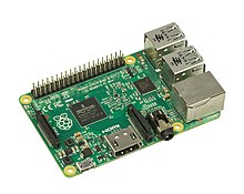
A system on a chip or system on chip (SoC or SOC) is an integrated circuit (IC) that integrates all components of a computer or other electronic system into a single chip. It may contain digital, analog, mixed-signal, and often radio-frequency functions—all on a single chip substrate. SoCs are very common in the mobile computing market because of their low power-consumption.[1] A typical application is in the area of embedded systems.
The contrast with a microcontroller is one of degree. Microcontrollers typically have under 100 kB of RAM (often just a few kilobytes) and often really are single-chip-systems, whereas the term SoC is typically used for more powerful processors, such as on smartphones.[2]:p.2SoCs are capable of running software such as the desktop versions of Windows and Linux, which need external memory chips (flash, RAM) to be useful, and which are used with various external peripherals. In short, for larger systems, the term system on a chip is hyperbole, indicating technical direction more than reality: a high degree of chip integration, leading toward reduced manufacturing costs, and the production of smaller systems. Many systems are too complex to fit on just one chip built with a processor optimized for just one of the system's tasks.
When it is not feasible to construct a SoC for a particular application, an alternative is a system in package (SiP) comprising a number of chips in a single package. In large volumes, SoC is believed[by whom?] to be more cost-effective than SiP since it increases the yield of the fabrication and because its packaging is simpler.[3]
Another option, as seen for example in higher-end cell phones, is package on package stacking during board assembly. The SoC includes processors and numerous digital peripherals, and comes in a ball grid package with lower and upper connections. The lower balls connect to the board and various peripherals, with the upper balls in a ring holding the memory buses used to access NAND flash and DDR2 RAM. Memory packages could come from multiple vendors.
Structure
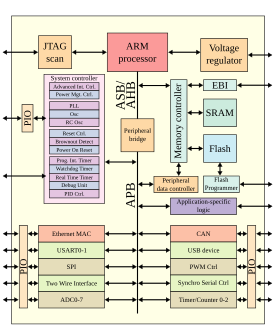
A typical SoC consists of:
- a microcontroller, microprocessor or digital signal processor (DSP) core – multiprocessor SoCs (MPSoC) having more than one processor core
- memory blocks including a selection of ROM, RAM, EEPROM and flash memory
- timing sources including oscillators and phase-locked loops
- peripherals including counter-timers, real-time timers and power-on reset generators
- external interfaces, including industry standards such as USB, FireWire, Ethernet, USART, SPI
- analog interfaces including ADCs and DACs
- voltage regulators and power management circuits
A bus – either proprietary or industry-standard such as the AMBA bus from ARM Holdings – connects these blocks. DMA controllers route data directly between external interfaces and memory, bypassing the processor core and thereby increasing the data throughput of the SoC.
Design flow
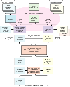
A SoC consists of both the hardware, described above, and the software controlling the microcontroller, microprocessor or DSP cores, peripherals and interfaces. The design flow for a SoC aims to develop this hardware and software in parallel.
Most SoCs are developed from pre-qualified hardware blocks for the hardware elements described above, together with the software drivers that control their operation. Of particular importance are the protocol stacks that drive industry-standard interfaces like USB. The hardware blocks are put together using CAD tools; the software modules are integrated using a software-development environment.
Once the architecture of the SoC has been defined, any new hardware elements are written in an abstract language termed RTL which defines the circuit behaviour. These elements are connected together in the same RTL language to create the full SoC design.
Chips are verified for logical correctness before being sent to foundry. This process is called functional verification and it accounts for a significant portion of the time and energy expended in the chip design life cycle (although the often quoted figure of 70% is probably an exaggeration).[4] With the growing complexity of chips, hardware verification languages like SystemVerilog, SystemC, e, and OpenVera are being used. Bugs found in the verification stage are reported to the designer.
Traditionally, engineers have employed simulation acceleration, emulation and/or an FPGA prototype to verify and debug both hardware and software for SoC designs prior to tapeout. With high capacity and fast compilation time, acceleration and emulation are powerful technologies that provide wide visibility into systems. Both technologies, however, operate slowly, on the order of MHz, which may be significantly slower – up to 100 times slower – than the SoC's operating frequency. Acceleration and emulation boxes are also very large and expensive at over US$1,000,000. FPGA prototypes, in contrast, use FPGAs directly to enable engineers to validate and test at, or close to, a system’s full operating frequency with real-world stimuli. Tools such as Certus[5] are used to insert probes in the FPGA RTL that make signals available for observation. This is used to debug hardware, firmware and software interactions across multiple FPGAs with capabilities similar to a logic analyzer.
In parallel, the hardware elements are grouped and passed through a process of logic synthesis, during which performance constraints, such as operational frequency and expected signal delays, are applied. This generates a logical netlist which is a file describing the circuit as a collection of connected silicon gate elements from a library provided by the silicon manufacturer.
This netlist is used as the basis for the physical design (place and route) flow to convert the designers' intent into the polygonal design of the SoC. Throughout this conversion process, the design is analysed with static timing modelling, simulation and other tools to ensure that it meets the specified operational parameters such as frequency, power consumption and dissipation, functional integrity vs. the RTL and electrical integrity.
When all known bugs have been rectified and these have been re-verified and all physical design checks are done, the physical design files describing each layer of the chip are sent to the foundry's mask shop where a full set of glass lithographic masks will be etched. These are sent to the wafer fabrication plant to create the SoC dice before packaging and testing.


No comments:
Post a Comment