Using tri-state logic
After reviewing all the learning to date I realised that I have failed to cover tri-state logic! Although common when building projects using individual chips it only really makes an appearance in FPGA designs when interfacing to external components (explaining why it was only seen when interfacing to the Basys2’s bidirectional EPP port).
What is tri-state logic?
Put simply, tri-state logic is where a signal can be either "logic high level", "logic low level" or "not actively driven" - 1, 0 and Z in VHDL. This allows the same wire / signal to be used as both an input or output, or allow multiple devices to "share" a common bus.
The most familiar example is a RAM chip’s data bus. During the read cycles the memory chip drives the data bus, and during write cycles the memory controller drives the data bus. To enable this, most RAM chips have a signal called "Output Enable" ("OE") that tells the chip when to drive the bus.
On a tri-state bus all devices on the bus can read the value of the bus at any time, but to avoid data corruption your design must ensure that one device should drive the bus at any time. Should two or more devices try to drive the bus to different values at the same time the data on the bus will be corrupted. If this overlap of multiple devices driving the bus lasts for only a short time then an error may not occur, but you will get increased power usage and signal integrity issues as the output drivers are saturated.
How is tri-state logic used within an FPGA
In short, for the Spartan 3E it isn’t. To avoid timing and power issues, the design tools ensure that any signals are only ever driven by one device.
Any internal tri-state logic within a design is mapped into hidden "input" and "output" signals. The bus is then implemented with a multiplexer that selects the active output signal and then delivers that signal to all the inputs.
How is tri-state logic is use when interfacing with an FPGA
Most general purpose I/O pins of an FPGA are driven by a tri-state driver, and the pin is monitored by an input buffer. When any internal tri-state signal is attached to an I/O pin it is implemented as three signals driving an IOBUF component:
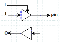
• T controls the state of the tri-state driver
• O is the value of the pin
• I is the value that will be sent to the pin when T is asserted
Yes, the signal names do seem the wrong way around, but they are from the IOBUF’s point of view.
Project - using tri-state logic
Sadly this project is Basys2 only - as on the Papilio One the LogicStart MegaWing uses all the I/O pins. It is possible to remove the MegaWing and connect directly to the headers on the Papilio One if you want. . .
• Create a new project
• Configure two of the PMOD pins. Remember to define the PMOD pins as "INOUT"!
• Have 2 LEDs show the status of the two pins on a PMOD connector,
led(0) <= pmod(0);
led(1) <= pmod(1);
• Connect two slide switches to these pins
pmod(0) <= sw(0);
pmod(1) <= sw(1);
• Put a 300 Ohm + resistor between the two pins (to limit the current if both pins are driven at once)
• Put a voltmeter across the resistor
• Play around with the design
– What is the highest voltage you can place over the resistor?
– How much power is this ( remember P=Vˆ2/R)
• Using a third slide switch decide which of the pins will be in high-Z mode. Something like:
process(sw)
begin
if sw(2) = ’1’ then
pmod(0) <= ’Z’;
pmod(1) <= sw(1);
else
pmod(0) <= sw(0);
pmod(1) <= ’Z’;
end if;
end process;
• Play around with it
– What is the highest voltage you can get over the resistor now?
– How much power is this?
No comments:
Post a Comment